
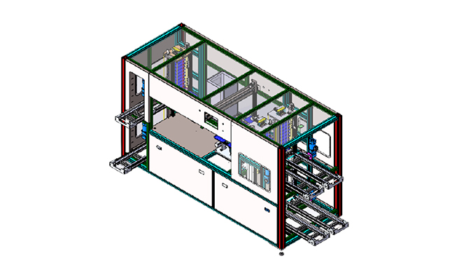
PL/EL/IR/IV TESTING SYSTEM
A high-precision inspection system used to evaluate solar cells and wafers through multiple imaging and analysis modes— Photoluminescence (PL), Electroluminescence (EL), Infrared (IR), and IV curve testing. It detects micro-cracks, defects, impurities, resistance issues, and electrical performance parameters.
The PL can be used after each manufacturing process like raw wafer, diffusion, deposition and printing. Ensures accurate quality grading, process optimization, and reliable efficiency measurement for PV manufacturing and R&D applications. Can be configured in any combination of EL/PL/IV/IR with manual and auto loading/unloading feature.
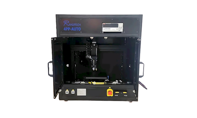
Four-Point Probe Measurement System
Experience high-precision electrical characterization with our Four-Point Probe Measurement System — engineered for accurate, low-resistance measurements of semiconductor wafers, thin films, and advanced materials. Its four-probe design eliminates contact resistance, delivering stable, repeatable results for sheet resistance, resistivity, and conductivity testing. Ideal for R&D labs and semiconductor, solar, and materials manufacturing, this system ensures reliable process control and superior material quality analysis. The system comes with auto axis control and mapping function.
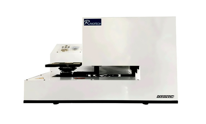
Spectroscopic Reflectometer
Achieve fast, accurate, and non-destructive thin-film analysis with our advanced Spectroscopic Reflectometer. Designed for precise measurement of film thickness, refractive index, and optical constants, it ensures exceptional performance across semiconductor, solar, LED, and materials research applications. With high-resolution spectral data and reliable repeatability, this tool enables superior process monitoring, quality control, and R&D innovation. The system comes with auto mapping function.
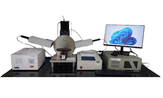
Ellipsometry Solutions
Unlock high-precision thin-film characterization with our advanced Ellipsometry Solutions. Engineered for accurate measurement of film thickness, refractive index, optical constants, and multilayer structures, our systems deliver unmatched sensitivity and repeatability. Ideal for semiconductor, photovoltaic, display, and materials research, these solutions provide powerful, non-destructive analysis to enhance process control, quality assurance, and R&D innovation. The system is suitable for TOPCON application (Including Tunnel Ox) and comes with various automation fu thenction based on user choice.
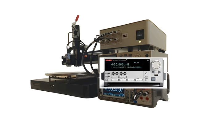
TLM Probe Measurement System
High-precision system for TLM contact resistance, sheet resistance, and Ag line resistivity on wafers up to 230 × 230 mm. Features a 14-pin Au/BeCu probe head with customizable layouts, full noise immunity, and smooth X-Y-Z motion. Includes a vacuum chuck for secure samples and shielded cabling for reliable signal integrity. Ideal for semiconductor fabs, PV, and R&D labs.
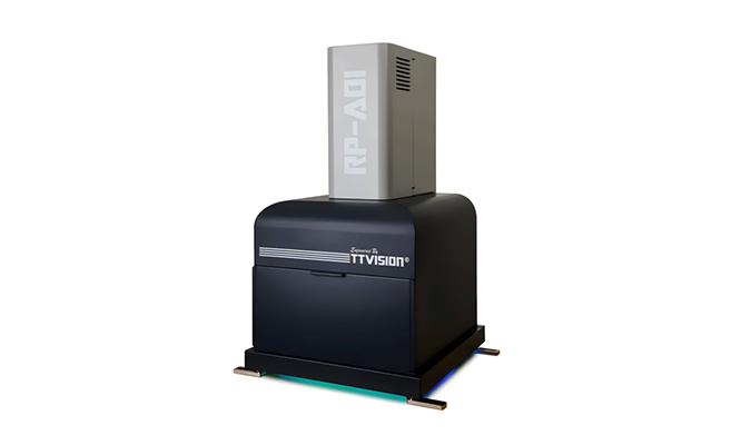
AOI (Automated Optical Inspection) System
Enhance quality and boost production efficiency with our high-precision AOI System. Designed for semiconductor, PCB, and electronics manufacturing, it detects defects in real time using advanced imaging and AI algorithms. Achieve faster inspection, higher accuracy, and reliable process control —ideal for modern, high-volume automated production lines. Suitable for applications in solar and semiconductor.
Get In Touch
-
B 109 & 111, 1st Floor, Tower-4 NX One Business Park, Techzone-4 Greater Noida West, UP (India)