
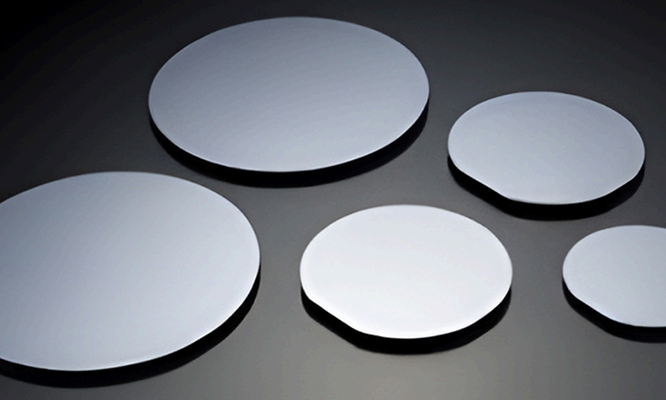
Epi Wafer (Epitaxial Wafer)
High-quality epitaxial wafers engineered for superior surface uniformity, low defect density, and stable electrical performance. Designed for advanced semiconductor devices, these epi wafers provide excellent doping control and thickness precision— ideal for power devices, high-speed ICs, RF
components, and optoelectronic applications. Perfect for manufacturers seeking reliable, high-purity epitaxial substrates that enhance device efficiency and yield

SiC Wafers (Silicon Carbide Wafers)
Premium SiC wafers engineered for highpower, high-temperature, and highfrequency applications. With superior thermal conductivity, wide bandgap performance, and excellent breakdown voltage, these silicon carbide wafers deliver unmatched efficiency for EV power modules, power electronics, RF devices, and industrial energy systems. Ideal for manufacturers seeking reliable, highquality SiC substrates with consistent surface quality and low defect density.
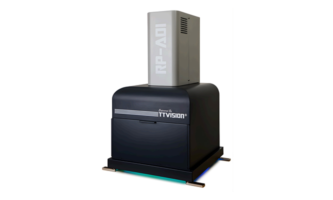
AOI (Automated Optical Inspection) System
Enhance quality and boost production efficiency with our high-precision AOI System. Designed for semiconductor, PCB, and electronics manufacturing, it detects defects in real time using advanced imaging and AI algorithms. Achieve faster inspection, higher accuracy, and reliable process control
—ideal for modern, high-volume automated production lines.
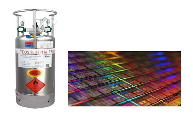
SPECIALITY GASES & CHEMICAL
High purity semi conductor grade chemical and gases like TEOS, TMB, TMP, TMPO, TEPO, TEB, K2CO3, TMA, POCL3
Get In Touch
-
B 109 & 111, 1st Floor, Tower-4 NX One Business Park, Techzone-4 Greater Noida West, UP (India)