
Spectroscopic Ellipsometry (SE) has become a cornerstone technique for thin-film characterization across semiconductor, photovoltaic, and advanced coating industries. It offers nanometer-scale precision in determining film thickness, refractive index (n), extinction coefficient (k), and even interface roughness — all non-destructively.
However, like any optical technique, the accuracy and reliability of results depend not only on the instrument, but also on how intelligently it’s applied. Let’s explore how to get the best out of spectroscopic ellipsometry through proven practices and real-world insights
1️⃣ Start with Clean, Flat, and Stable Samples
- Surface cleanliness is critical. Dust, oil, fingerprints, or moisture can scatter or depolarize reflected light.
- Use cleanroom-grade wipes and solvents like IPA or acetone before measurement.
- Ensure the sample is flat and stable — mechanical vibrations or warping can introduce angular misalignment and fitting errors.
- For multi-layer samples, verify uniformity across the wafer or substrate area.
Even a 1 nm surface film of organic residue can alter ellipsometric Ψ and Δ by 0.1–0.5°, shifting thickness estimates by several nanometers.
2️⃣ Choose the Right Spectral Range
Ellipsometers typically operate from UV to NIR (190–1700 nm) or UV–MIR (up to 5000 nm) depending on the system.
- A typical solar cell multilayer (e.g. SiNx, Al₂O₃, SiO₂) benefits from a 250–1100 nm range for accurate modeling.
- Use UV range to probe electronic transitions and bandgap edges in semiconductors (e.g. Si, GaAs).
- NIR region is useful for optical coatings and polymers where absorption is low.
- Broader spectral ranges improve dispersion modeling and reduce parameter correlation between n, k, and thickness.
3️⃣ Measure at Multiple Angles of Incidence
Each angle provides different sensitivity to film parameters.
- Higher angles (70°–75°) increase sensitivity to thin films and refractive index.
- Lower angles (55°–60°) are better for thicker layers.
- Photovoltaic (Solar Cell) application like multilayers on a textured surface typically works with 70°–75°
Studies show correct angle measurements can reduce thickness error by up to 50%.
4️⃣ Build Accurate Optical Models
Spectroscopic Ellipsometry doesn’t measure thickness/RI directly — it infers it by fitting experimental data to an optical model. So creating the right model is essential.
- Use Cauchy models for transparent dielectrics,
- Tauc–Lorentz or Forouhi–Bloomer models for semiconductors,
- and Drude models for metals or conductive films.
- Constrain models using known literature data or complementary measurements (AFM, SEM, XRR).
- Always check mean square error (MSE) of the fit — lower is better, but physical realism matters more.
A good ellipsometric model balances mathematical accuracy and physical meaning — not just a low MSE.
5️⃣ Validate with Complementary Techniques
Cross-validation ensures your model isn’t just fitting noise. Combine SE with:
- AFM → surface roughness verification
- SEM/TEM cross-section → interface validation
- X-ray Reflectivity (XRR) → thickness calibration
- Spectrophotometry → transmission/reflectance matching
For optical coatings, SE + XRR correlation often yields < 1% thickness deviation.
6️⃣ Automate and Standardize Measurements
In R&D and production, repeatability is as crucial as accuracy.
- Use automated mapping for wafer-scale uniformity checks.
- Create measurement recipes with fixed angles, spectral range, and model templates.
- Integrate auto-focus and feedback correction for faster, error-free operation.
- In-line or real-time SE systems (used in CVD or ALD processes) can monitor film growth dynamics and optimize deposition in real time.
- Choosing a correct measurement recipe is crucial, verify your layers before creating the recipe.
- Regularly tune the recipe models to correspond to the change in process.
In advanced fabs, automated SE improves throughput and reduces operator dependence — a must for production metrology.
7️⃣ Train and Continuously Calibrate
Ellipsometry is model-driven, so expertise matters as much as hardware.
- Train your team on optical physics, model fitting, and uncertainty analysis.
- Routinely calibrate the system using reference Si wafers or SiO₂ standards.
- Update dispersion models as new materials or deposition processes are introduced.
Regular calibration ensures measurement stability within ±0.1 nm over months of operation.
8️⃣ Ellipsometery for Solar Cell application
In Solar application it uses a semi polished and textured surface of the Si wafer . Texturing roughens the surface to reduce reflection by increasing light trapping, which is significant for solar cell efficiency. This makes the ellipsometer measurement more complicated. Following tricks helps :
- Control texture height and angle parameters carefully, as these influence optical performance and measurement quality.
- Sample Alignment: Align the textured surface carefully using tilted and rotated sample stages to maximize signal quality due to non-flat surface geometry.
- Measurement Speed and Resolution: Adjust measurement speed to balance between high spectral resolution and avoiding signal blurring due to surface roughness. Faster measurements may be needed for in-situ monitoring but slower measurements increase accuracy.
- Employ high-intensity light sources and intensity optimization to overcome reflection losses caused by texture.
- Use thick layers to get good accuracy and repeatability. Adjust process parameters and optimize the process accordingly.
- Advanced Optical Modeling: Advanced modeling techniques allow the study of complex multilayer and textured structures to extract optical constants and thicknesses accurately, even on rough surfaces.
Regular recipe model optimization helps in accurate data extraction. Don’t forget to provide a careful handling of your equipment.
✅ Key Takeaways
| Step | Action | Impact |
| Clean, flat sample | Remove contaminants | Prevents optical distortion |
| Multi-angle, wide spectrum | Broader data set | Reduces model correlation |
| Physically accurate models | Cauchy / Tauc-Lorentz | Reliable parameter extraction |
| Cross-validation | AFM / XRR / SEM | Confidence in results |
| Automation | Recipes & feedback | High throughput, reproducibility |
| Regular calibration | Standard references | Long-term accuracy |
STEP, ACTION & IMPACT OF BEST SPECTROSCOPIC ELLIPSOMETRY
🌟 Conclusion
To get the best out of Spectroscopic Ellipsometry, treat it as more than just a measurement tool — it’s an analytical ecosystem. When you combine clean samples, smart spectral strategy, robust modeling, and expert interpretation, SE delivers unmatched insight into material properties and process control.
In research, it accelerates innovation. In production, it safeguards consistency. And when optimized correctly — it remains the most precise, non-destructive window into the nanoscale world.
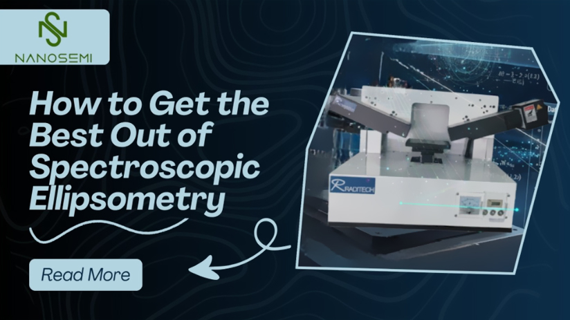
Our partner Raditech – Taiwan is a prominent supplier of the Spectroscopic Ellipsometer, best suited for the production environment in Solar & Semiconductor.
To know more please connect here
880-050-5033 | sales@nanosemi.in