
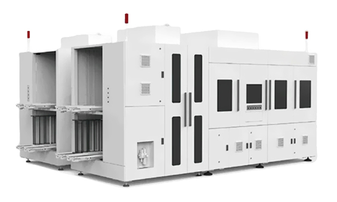
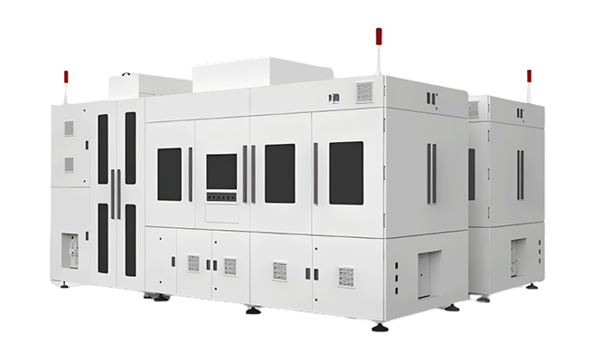
xBC Cell Laser Contact Opening
Our laser film opening equipment features an advanced optical path design that enables high-speed, high-efficiency film opening with exceptional cell patterning accuracy. Designed for full compatibility with both N-type and P-type silicon substrates, this system significantly reduces back-side metal line resistance while enhancing contact performance. The result is superior electrical conductivity and excellent passivation capabilities, ensuring higher cell efficiency and more reliable manufacturing outcomes.
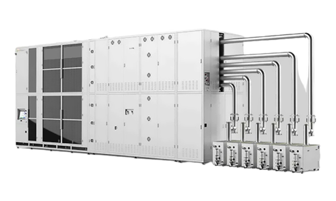
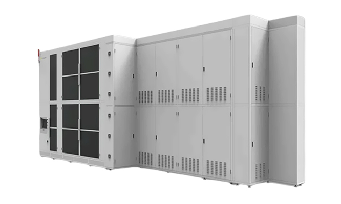
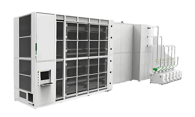
Low Pressure Chemical Vapor Deposition
Our system utilizes a low-pressure thermal decomposition process to form highquality silicon oxide and a range of crystalline silicon films. Designed to meet the demanding requirements of tunneling oxidation passivation, it delivers exceptional uniformity and stability for advanced solar manufacturing. This technology is perfectly suited for producing high-efficiency N-type TOPCon and BC solar cells, ensuring superior passivation performance, enhanced cell efficiency, and reliable production for next-generation photovoltaic applications.fytft
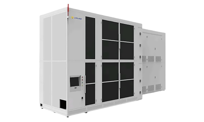
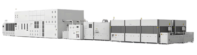
Low Pressure Oxidation / Annealing
The low-pressure horizontal oxidation and annealing system is designed for highprecision thermal annealing and thermal activation processes across a wide range of solar cell structures. Engineered for versatility and stable performance, it supports advanced cell technologies including PERC, PERT, TOPCon, and BC. With uniform temperature control and optimized process conditions, this system ensures superior film quality, improved passivation, and enhanced efficiency for next-generation photovoltaic manufacturing.
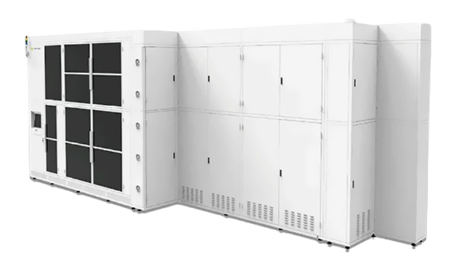
Low Pressure Horizontal Placement Boron Diffusion Equipment
Through high-temperature thermal decomposition and controlled chemical reactions, this system enables the precise growth of borosilicate glass (BSG) while achieving effective boron diffusion anddoping. Designed for advanced photovoltaic manufacturing, it delivers stable and uniform processing for silicon wafer oxidation and boron doping applications. This ensures high-quality surface passivation, optimized dopant profiles, andimproved performance for next-generation solar cell technologies.fytft
Low Pressure POCL Diffusion
Through high-temperature thermal decomposition and controlled chemical reactions, the system enables the deposition of phosphosilicate glass (PSG) along with the precise diffusion and doping of phosphorus atoms. It is widely used for silicon wafer oxidation, phosphorus doping, poly-phosphorus doping, and other advanced semiconductor and solar cell processes. With uniform film formation and stable dopant control, the system ensures high-quality surfaces, optimized electrical properties, and enhanced performance for next-generation photovoltaic applications.
Atomic Layer Deposition System
By alternately introducing gas-phase precursor pulses into the reactor, the material is absorbed onto the substrate surface and reacts to form a uniform, high-quality deposited film. This precise and self-limiting reaction mechanism makes the process ideal for advanced photovoltaic manufacturing, especially for TOPCon solar cell applications, where superior passivation, film conformity, and process stability are essential for achieving high cell efficiency.
Atomic Edge Passivation Deposition Complete Solution
Laser non-destructive etching uses precise laser heating combined with localized cooling to create astrong temperature gradient within the silicon wafer. This gradient induces controlled thermal stress that reaches the fracture threshold, allowing the crack to propagate cleanly along the laserdefined path. As a result, the material separates completely without mechanical force, ensuring high-precision cutting, minimal damage, and superior edge quality—ideal for advanced solar cell and semiconductor manufacturing.
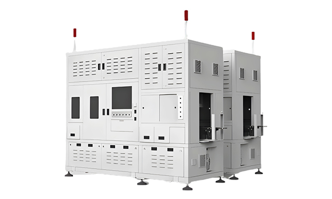
Laser Induced Metallization Equipment
This technology uses a highly precise laser process to selectively remove the passivation layer on the surface of silicon wafers, enabling optimized metal contact and significantly reduced contact resistance. By improving electrical connection quality, it effectively enhances the conversion efficiency of solar cells. The system is fully compatible with advanced manufacturing processes, including TOPCon, xBC, half-cell, threecell, and 0BB architectures, making it ideal for nextgeneration high-efficiency photovoltaic production.
Poly Thickness Reduction via Laser Abl/ Laser Induced Oxidation
This TOPCon cell development equipment utilizes ultrafast laser ablation to precisely remove the rear-side PSG layer, followed by controlled wet etching to thin the polysilicon layer. By minimizing parasitic light absorption at the rear polysilicon interface, the process significantly enhances optical performance while reducing material usage. This dual optimization enables lower manufacturingcosts and improved cell efficiency, making it an ideal solution for next-generation high-efficiency TOPCon solar cell production.
Plasma Enhanced Chemical Vapor Deposition
This system uses high-temperature discharge to ionize gas into plasma, enabling efficient reaction and film deposition. It supports the preparation of multiple high-performance thin films, including silicon carbide, silicon nitride, silicon oxynitride, and aluminum oxide. Engineered for advanced photovoltaic manufacturing, it is ideal for a wide range of cell technologies such as PERC, PERT, TOPCon, and BC, ensuring excellent surface passivation, superior film quality, and improved overall cell efficiency.
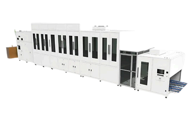
Mono-Si Texturing Cleaning Equipment
This system leverages the anisotropic alkali reaction of silicon to form uniform pyramid structures on wafer surfaces, enhancing lighttrapping for higher solar cell efficiency. The processflow includes Rough Polishing → Pre-cleaning → Texturing → Post-cleaning (O₃ compatible) → Pickling→ Pre-dehydration → Drying. Features include adjustable etching depth, support for MES and RFID, optional online weighing, one-key cleaning, online slot replacement, and adjustable process tank circulation for simple, efficient operation and optimized wafer processing
Inline BSG Removal Equipment
Function: Removing Boron Silicate Glass (BSG) fromPhotovoltaic Solar Cells
This equipment is designed for precise removal of Boron Silicate Glass (BSG) from photovoltaic solar cells, following the process flow: Water Film → HF → Water Film → HF → Rinse → Drying. It features a highspeed precision liquid-carrying etching roller to prevent under- or over-etching at wafer edges, along with accurate water film control for completecoverage without dripping. Real-time solution conductivity monitoring ensures process stability, while stable production at 4.5m/min, low friction, and extended consumable life deliver efficient and reliable BSG etching for advanced solar cell manufacturing.
Mono-Si Alkaline Polishing Equipment
This system provides precision polishing for silicon wafer surfaces, following the process flow: Precleaning → Polishing → Post-cleaning → Pickling → Pre-dehydration → Drying. It supports MES, RFID, and optional online weighing, with one-key online washing and solution replacement for fast and easyfluid exchange. The adjustable process circulation volume and compatibility with additives from various brands ensure consistent, high-quality polishing results, making it ideal for advanced solar cell manufacturing.
Inline PSG Removal Equipment
This equipment is designed for accurate removal of Phosphorus Silicon Glass (PSG) from photovoltaic solar cells, following the process flow: Water Film → HF → Rinse → Drying. It features a high-speed precision liquid-carrying etching roller to prevent under- or over-etching at wafer edges, along with precise water film control for complete coverage without dripping. Real-time solution conductivity monitoring ensures stable etching performance, while production at 4.5m/min, low friction, and extended consumable life provide efficient, reliable, and consistent PSG removal for advanced solar cell manufacturing.
RCA Cleaning Equipment
This system is designed for the precise removal of LPCVD/PECVD deposited polysilicon from silicon wafers, following the process flow: Deposition Removal → Post-cleaning → Pickling → Post-cleaning. It supports MES, RFID, and optional online weighing,with one-key online washing and solution replacement for fast and easy fluid exchange. The adjustable process tank circulation volume and compatibility with additives from various brands ensure thorough deposition removal, complete cleaning, and consistent high-quality results, making it ideal for advanced solar cell manufacturing.
BOE Cleaning Equipment
This system enables efficient removal of PSG and silicon oxide in PVD processes, using the flow: Pickling → Rinse → Pre-dehydration → Drying. It supports MES, RFID, and optional online weighing, with one-key online washing and fast solution replacement for easy operation. Adjustable tank circulation and compatibility with multiple additivebrands ensure thorough deposition removal and clean, consistent wafer processing.
Get In Touch
-
B 109 & 111, 1st Floor, Tower-4 NX One Business Park, Techzone-4 Greater Noida West, UP (India)